What data recovery tools to buy if you want to start a data recovery business?
Free video data recovery training on how to recover lost data from different hard drives?
Where to buy head and platter replacement tools at good prices?
Data recover case studies step by step guide
I want to attend professional data recovery training courses
The physical mechanism to store data in flash memory is based on storing electrical charge into a floating gate of a transistor. This charge can be stored for extended periods of time without using an external power supply but gradually it will leak away caused by physical effects. Data retention specifications for current flash memory are between 10 and 100 years.
Flash memory can be written byte for byte, like EEPROM , but it has to be erased in blocks at a time before it can be
re-written. Erasing results in a memory block that is filled completely with 1’s. In NAND flash, erase blocks are divided further into pages, for example 32 or 64 per erase block. A page is usually a multiple of 512 bytes in size, to emulate 512 byte sector size commonly found in file systems on magnetic media. Additionally, a page has a number of so called ’spare area’ bytes, generally used for storing meta data.
Some flash disk drivers use the concept of zones . A zone is a group of blocks, usually 256 to 1024. Contrary to blocks and pages, a zone is just a logical concept, there is no physical representation. See figure 1 for a dissection of NAND flash memory.
SMALL SCALE DIGITAL DEVICE FORENSICS JOURNAL, VOL. 1, NO. 1, JUNE 2007
figure 1: Dissection of NAND flash memory
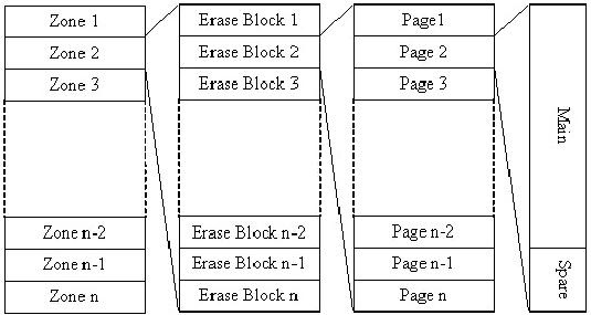
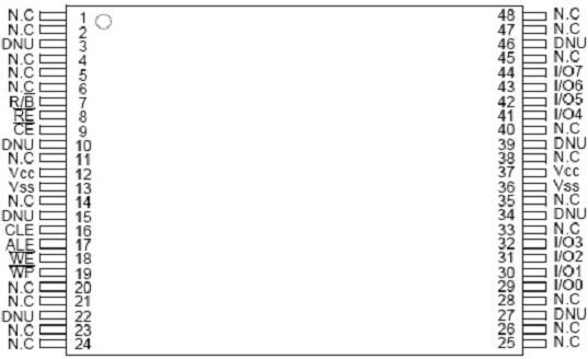
Fig. 2. Typical electrical interface of a NAND flash chip
TABLE I
EXAMPLE SPARE AREA SIZES FOR DIFFERENT PAGE SIZES (IN BYTES)
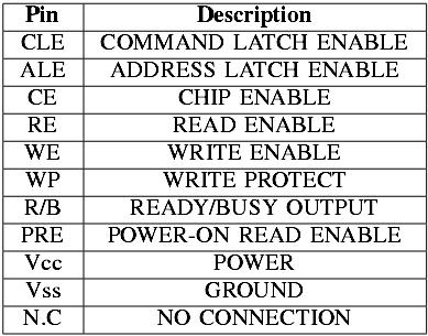
TABLE II : PIN NAMES OF A NAND FLASH CHIP
TABLE III: TYPICAL ADDRESSING CYCLES FOR A NAND FLASH CHIP
Each page has an area of bytes, often referred to as the redundant area or spare area. Table I shows spare area sizes
for different page sizes.The spare area can contain information on the status of the block or the page. For instance when a block turns bad,it will be markedhere.The spare area can also contain ECC data. ECC data is used to detect errors in a page. With the ECC data an error of one bit can be corrected, after which the block will be marked bad. Finally the spare area can contain information necessary for the physical to logical address mapping Erasing a block causes a block to deteriorate. Blocks can be erased between 10^4 and 10^6 times before bits in this block
start to become inerasable (stay ‘0’). Such a block is then called a ‘bad block’. NAND flash usually already has bad
blocks when leaving the factory. In datasheets of NAND flash chips, the guaranteed minimal number of good blocks when first shipped is specified. Typically at least 98% of the blocks are guaranteed to be in working order. Initial bad blocks are marked as such in the spare area.
In order to spread the erasing of blocks as evenly as possible over the full range of physical blocks, flash memory vendors have developed so called ‘wear levelling’ algorithms. The idea is that spreading the wear, caused by erasing a block, as much as possible over the whole capacity of the flash memory will increase the overall lifetime of the memory. For manufacturers of memory devices, the wear levelling algorithm can be very sensitive intellectual property, so any inquiries that look like questions about the wear levelling algorithm will often be left unanswered.
However, for the reconstruction of data in a flash memory, it is not necessary to know how the wear levelling created the physical image that is copied of a flash chip. All one needs to know is how to recreate the right order of physical blocks in order to create a logical copy of the higher level file system.In other words: wear leveling can be seen as a dynamic process that rearranges pages and/or blocks continuously in order to extend flash lifetime. When trying to interpret a static ‘snapshot’ of the wear leveling process (the exact binary copy of the physical flash memory at one particular moment) no knowledge of the ‘dynamic behavior’ of the wear leveling algorithm is needed.
The electrical interface of NAND flash differs from that of RAM. NAND flash has a multiplexed address/data bus,
generally referred to as the I/O (Input/Output) lines. This bus can be either 8 or 16 bits wide. An example of the electrical interface of a NAND flash chip is shown in figure 2, with the pin names in table II. Data in the NAND flash chip is accessed by first applying the address of the required data on the I/O lines. As the highest address is generally higher than can be reached with 8 or 16 I/O line bits, the address is latched into the chip in three to five address cycles. After the address is latched into the chip, the data can be clocked out over the same I/O lines. A typical sequence to get access to data in a NAND flash chip is shown in table III.
Data recovery Salon welcomes your comments and share with us your ideas, suggestions and experience. Data recovery salon is dedicated in sharing the most useful data recovery information with our users and only if you are good at data recovery or related knowledge, please kindly drop us an email and we will publish your article here. We need to make data recovery Salon to be the most professional and free data recovery E-book online.






Comments are closed
Sorry, but you cannot leave a comment for this post.